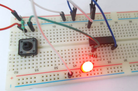
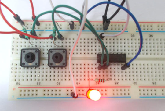
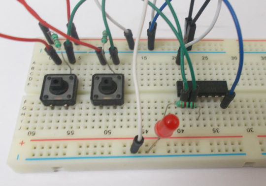
If you are diving into digital electronics, and you might have came across latches. In digital electronics, computers remember things with the help of simple circuits called latches which are the simplest memory elements. They store a single bit of binary data and play a key role in sequential circuits and memory design. One of the most fundamental types is the SR Latch (Set-Reset Latch), which operates with two inputs, Set (S) and Reset (R).
In this article, we will explore what an SR latch is, how it works, its truth table, and the differences between the basic SR Latch, Gated SR Latch, and Clocked SR Latch (SR Flip-Flop).
What is an SR Latch?

The SR Latch is a basic circuit that stores one bit of information. It has two inputs:
- Set (S): Makes the output high (
Q = 1) - Reset (R): Makes the output low (
Q = 0)
Once set, the output remains stable even if the inputs are removed, which is why it’s used as a memory element.
SR latches can be built using NOR gates or NAND gates. The only difference is that the NAND version uses active LOW inputs, while the NOR version works with active HIGH inputs.
Gated SR Latch
The Gated SR Latch is similar to the basic SR latch but includes an Enable input.
-
When Enable = 1, the latch responds to S and R inputs.
-
When Enable = 0, the output stays unchanged, regardless of inputs.
This provides more control and is often used in situations where the latch should only update at specific times.

Clocked SR Latch (SR Flip-Flop)
When a clock signal is introduced, the SR latch becomes edge-triggered, and is commonly called an SR Flip-Flop.
Here’s how it works:
-
S = 1, R = 0 → Q = 1 (Set)
-
S = 0, R = 1 → Q = 0 (Reset)
-
S = R = 0 → Previous state (No change)
-
S = R = 1 → Invalid condition
The clock ensures that the output only changes on a rising or falling edge, making it more reliable for sequential circuits.

Applications of SR Latch
- Basic memory storage elements
- Control circuits in microcontrollers and processors
- Debouncing switches in digital systems
- Building blocks for more advanced flip-flops (D, JK, T)