Showing posts with label HardwareDesign. Show all posts

Wednesday, 5 June 2024

Explore the fundamentals of Full Adder circuits


Binary adders come in two types: Half Adders and Full Adders. A half adder adds 2-bit binary numbers but cannot include a carry bit. In contrast, a Full Adder adds the carry bit along with the two binary numbers, enabling the addition of multi-bit binary numbers by cascading multiple Full Adder circuits.


Full Adder Circuit

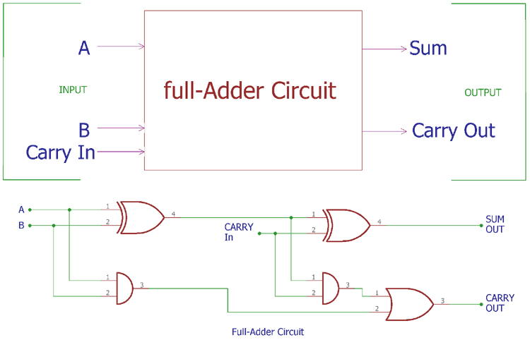
The main limitation of a half adder is the lack of a ‘Carry in’ bit. In a Full Adder circuit, we include a carry in input and add it to inputs A and B, giving us three inputs (A, B, and Carry In) and producing two outputs (SUM and Carry Out).


Full Adder Block Diagram

The Full Adder is constructed by combining two half-adder circuits and an OR gate. Here’s how it works:


  1. The first half-adder adds inputs A and B, producing SUM and Carry out.

  2. The SUM output from the first half-adder is fed into the second half-adder along with the Carry in bit.

  3. The final SUM output is the result of the Full Adder.

  4. The Carry out bits from both half-adders are combined using an OR gate to produce the final Carry out.


Construction of Full Adder Circuit

Here’s a step-by-step guide to constructing a Full Adder Circuit:


Components Needed

  • Two Half Adder circuits

  • OR Gate

  • Steps

  • Connect the inputs A and B to the first half-adder.

The SUM output from the first half-adder goes to the input of the second half-adder along with the Carry in bit.

The final SUM output from the second half-adder is the overall SUM output of the Full Adder.

Combine the Carry out bits from both half-adders using an OR gate to produce the final Carry out.


Circuit Diagram and Logic Gates

The full adder circuit utilizes XOR, AND, and OR gates. The two half adders are connected such that the first half adder handles inputs A and B, while its SUM output and the Carry in bit are fed into the second half adder. The OR gate then combines the Carry out bits from both half adders.


Truth Table of Full Adder Circuit

The truth table for the Full Adder circuit includes three inputs (A, B, Carry In) and two outputs (SUM, Carry Out):


The SUM output is obtained by XORing inputs A and B and then XORing the result with the Carry in bit. The Carry out is calculated by ORing the AND results of the input pairs.


Cascading Adder Circuits

To add multi-bit binary numbers, you can cascade Full Adder circuits, forming what’s known as a Ripple Carry Adder circuit. The Carry out from each Full Adder is connected to the Carry in of the next Full Adder, allowing the addition of larger binary numbers. However, this can introduce propagation delays, which can be mitigated using a carry look-ahead adder.



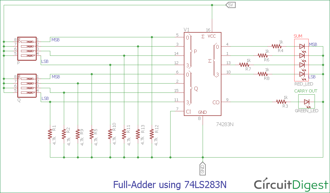
Practical Demonstration: Full Adder Using IC 74LS283N

To demonstrate a practical Full Adder, we use the IC 74LS283N, a 4-bit full adder with carry look-ahead features. Here’s a list of components required:

  • 74LS283N IC

  • 4-pin DIP switches (2 pcs)

  • Red LEDs (4 pcs)

  • Green LED (1 pc)

  • 4.7k resistors (8 pcs)

  • 1k resistors (5 pcs)

  • Breadboard

  • Connecting wires

  • 5V adapter


Circuit Setup

Connect the VCC and Ground to pins 16 and 8, respectively.

Connect the first 4-bit number to pins 5, 3, 14, and 12 (P inputs).

Connect the second 4-bit number to pins 6, 2, 15, and 11.

The SUM outputs will be on pins 4, 1, 13, and 10.

Use 4.7k resistors on all input pins to set logic 0 when switches are off.

Use red LEDs for SUM outputs and a green LED for the Carry out bit.

For a visual demonstration, check out the video tutorial below where we show adding two 4-bit binary numbers using the 74LS283N IC.


Understanding Full Adder circuits is crucial for digital electronics. By combining half adders and using logic gates, we can build efficient circuits for adding binary numbers, with applications ranging from simple calculators to complex computer systems.


Watch the detailed video tutorial here: Full Adder Circuit Tutorial.


Friday, 17 May 2024

Design Tips and Troubleshooting Guide for MCP2200 Protocol Converter

 The MCP2200, developed by Microchip Technology, serves as a USB-to-UART serial converter, facilitating the conversion of USB connections to serial interfaces.


Design Considerations


  • Ensure proper connectivity and voltage levels between the MCP2200 and connected devices.

  • Strategic placement of the USB port close to the IC for efficient data transfer.

  • Direct routing of data lines and minimal use of vias to reduce signal interference.

  • Include filter capacitors and maintain tight component arrangement to optimize performance.


Troubleshooting Tips


  • Verify signal connections and check voltage compatibility to address communication failures.

  • Test functionality by matching serial settings with connected devices and performing a loopback test for data transmission.

  • Use alternative USB cables to rule out potential cable issues.


Microcontroller programming, debugging, industrial control systems, DIY electronics projects, legacy device support, automation, and robotics. Alternatives include CH340, MA112AS16, FT230x, CP2102, PL2303HX, CH9102, CH343, CH341, CP2110, and FT232.


Detailed mechanical drawings and dimensions aid in creating custom footprints for PCB or CAD modeling, ensuring accurate integration of the MCP2200 into electronic designs. For detailed technical specifications and mechanical drawings, refer to the MCP2200 datasheet available here.


Thursday, 16 May 2024

Understanding the CH341: A Practical Guide to Design, Troubleshooting, and Applications

 The CH341 is a USB-to-serial UART converter chip designed by WCH (Nanjing QinHeng Corp), offering convenience and cost-effectiveness for embedded systems and microcontroller communication. It facilitates USB connectivity between circuits and computers, supporting USB 1.1 and USB 2.0 compatibility. With versatility in protocols like UART, I2C, SPI, and parallel interfaces, it's widely used for various applications.


Troubleshooting Tips for CH341


  • Ensure correct connections between the chip and other components.

  • Check compatibility of signal voltage levels with connected devices.

  • Verify integrity of the USB cable for data transmission reliability.

  • Utilize ready-made programmers for programming EEPROMs directly with CH341.


Design Considerations for PCB Layouts


  • Place decoupling capacitance near the chip pins to stabilize power supply.

  • Align D+ and D- data lines in parallel with adequate ground or copper pour.

  • Minimize signal lead lengths between XI and XO pins to reduce clock disturbances.

  • Optimize placement of USB port near the CH341 chip and route data lines efficiently.


Applications of CH341 span microcontroller programming, debugging, industrial control systems, DIY electronics projects, legacy device support, and various conversions like USB to RS485, RS232, and TTL serial port. Its footprint and dimensional information aid in creating custom footprints for PCB design and CAD modeling, ensuring optimal integration into systems. For detailed technical specifications and mechanical drawings, refer to the CH341 datasheet available here.


Tuesday, 14 May 2024

Exploring the CH9102 USB to Serial Converter: Design and Troubleshooting

 The CH9102 stands out as a robust USB to serial UART converter, engineered by WCH (Nanjing QinHeng Corp), widely adopted in USB-to-serial adapter cables and development boards. This article delves into its design aspects and offers troubleshooting insights for smoother integration into projects.


Troubleshooting Tips:


  • Verify Connections: Double-check all connections to ensure they are properly made between the CH9102 and other components of the circuit.

  • Check Signal Voltage Compatibility: Ensure that the voltage levels of the signals (TX, RX, etc.) are compatible with the devices you are connecting to.

  • Test Serial Settings: Align serial settings, such as baud rate, between your computer and the device you are communicating with to ensure compatibility.

  • Conduct Loopback Test: Perform a loopback test by connecting the TX and RX pins of the CH9102. Send data from your computer, and if it is received correctly, it indicates that the CH9102 is functioning properly.

  • Address Computer Recognition Issues: Install correct drivers for the CH9102 chip on your computer. Check for hardware connection problems in the Device Manager, ensuring the chip is recognized without any error messages.


Design Considerations:


  • Strategic USB Port Placement: Place the USB port near the CH9102 IC on the PCB layout to minimize signal interference and optimize data transfer.

  • Direct Routing of Data Lines: Route data lines directly to reduce signal degradation and improve overall signal integrity.

  • Minimal Via Count: Minimize the number of vias in data lines to avoid signal loss and maintain signal integrity.

  • Inclusion of Filter Capacitors: Incorporate filter capacitors to stabilize voltage and reduce noise, enhancing the performance of the CH9102 and surrounding components.

  • Comprehensive Component Arrangement: Arrange components strategically to optimize space utilization and ensure efficient heat dissipation, contributing to the stability and reliability of the overall system.


Applications:

The CH9102 finds versatile applications in microcontroller programming, industrial control systems, DIY electronics projects, and legacy device support. Its adaptability extends to USB to RS485, RS232, and TTL serial port conversions, making it indispensable across various domains. 

Alternatives to CH9102 include CP2102, CP2104, CH340, MA112AS16, FT230x, PL2303HX, CH341, CH343, MCP2200, CP2110, and FT232.


As a cornerstone in USB connectivity solutions, the CH9102 offers reliability and efficiency. Understanding its design intricacies and troubleshooting methods ensures optimal performance in diverse project scenarios, making it a preferred choice for engineers and enthusiasts alike. For detailed technical specifications and mechanical drawings, refer to the CH9102 datasheet available here.